
Instruire & Consultanta
 Courses
3. Circuit Simulation (PSpice)
3.1  OrCAD PSpice, basic level
Course Contents
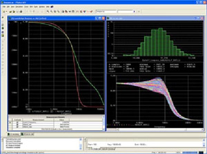
The course provides the participants with an overview of schematic design and circuit simulation and presents, based on numerous case studies and examples, a practical approach on development and optimizing of electronic projects based on circuit simulation. It presents fundamentals of schematic design and circuit simulation. Some Flash movies, which are destined to a better understanding of simulation flow, are also presented.
Course Duration
2 days - 1.5 days for the course and 0.5 day for performance evaluation, remarks and final discussions.
Course Outline
DAY 1
- Setup & management of OrCAD PSpice projects.
- Interfacing OrCAD Capture & OrCAD PSpice.
- Signal and power supply sources: types and fields of application.
- Introduction to Probe (traces, markers, zoom of signals, cursors, labelling & marking).
- DC analysis.
- Basics of time domain (transient) analysis.
- Basics of AC analysis.
DAY 2
- Parametric analysis & temperature analysis.
- Basics of digital simulation (sources, signals, digital devices and circuit analysis).
- Course summary/review
- Multiple-choice test for the theory
- Practice exam
- Instructor/student conference with technical remarks and final discussions
Course Notes
A set of course notes and various printed technical documents will be provided to each participant.
Fee
500 EUR/company, unlimited number of participants
- For independent specialists the fee can be lower, based on negotiations.
Performance Evaluation
A final exam will be used at the end of the course to evaluate the performance. The exam is divided in two parts, one multiple-choice test for the theory and one practice exam focused on engineering aspects of the course.
Who should attend
The course is designed for electrical and electronics managers and leaders involved in supervising schematic and PCB design, engineers, professors in the field of electronic packaging, and students who wish to get an overview of schematic design and to learn more about the design flow. The course is focused on various practical aspects and, due to a large number of examples which can be directly applied in practice, is addressed to people who want to learn quickly the basics of PCB design.
3.2 OrCAD PSpice, standard level
Course Contents
The course provides the participants with a systematic overview of schematic design and circuit simulation and presents, based on numerous figures, case studies and examples, a practical approach on development and optimizing of electronic projects based on PSpice circuit simulation. The chapters cover a large area of topics, from fundamentals of schematic design to simple or complex simulations, based on various practical projects. Some Flash movies, which are destined to a better understanding of schematic design flow and PSpice simulation, are also presented.
Course Duration
3 days - 2.5 days for the course and 0.5 day for performance evaluation, remarks and discussions.
Course Outline
DAY 1
- Setup & management of OrCAD PSpice Projects.
- Advanced interfacing between OrCAD Capture & OrCAD PSpice.
- Signal and power supply sources: types and fields of application.
- Introduction to Probe (traces, markers, zoom of signals, cursors, labelling & marking).
- DC analysis:
 bias point (passive & active structures) and
DC sweep (I-V characteristic, DC transfer curves, temperature analysis).
bias point (passive & active structures) and
DC sweep (I-V characteristic, DC transfer curves, temperature analysis). - Time domain (transient) analysis (sources, maximum step size, convergence, circuits with BJTs, circuits with integrated circuits).
DAY 2
- AC sweep analysis (magnitude and phase, Bode plots, amplifier gain analysis).
- Parametric analysis (variable devices, maximum power transfer, parametric sweep).
- Temperature analysis (variable working temperatures, temperature sweep).
- Working with the Stimulus Editor.
DAY 3
- Editing models (changing the reference, modifying existing models, downloading models from manufacturers).
- Digital simulations (sources, signals, digital devices and circuits analysis).
- Course summary/review
- Multiple-choice test for the theory
- Practice exam
- Instructor/student conference with technical remarks and final discussions
Course Notes
A set of course notes and various printed technical documents will be provided to each participant.
Fee
800 EUR/company, unlimited number of participants
- For independent specialists the fee can be lower, based on negotiations.
Performance Evaluation
A final exam will be used at the end of the course to evaluate the performance. The exam is divided in two parts, one multiple-choice test for the theory and one practice exam focused on engineering aspects of the course.
Who should attend
The course is designed for electrical and electronics engineers involved in schematic and PCB design, professors in the field of electronic packaging, technical managers, and students who wish to get a comprehensive overview of schematic design of electronic projects and to learn more about various applications. The course is focused on various practical aspects and, due to a large number of examples and case studies which can be directly applied in practice, is addressed also to R&D engineers and researchers from innovative companies involved in development of high performance electronic products.
3.3 OrCAD PSpice, advanced level
Course Contents
The course provides the participants with a systematic overview of schematic design and circuit simulation and presents, based on numerous figures, case studies and examples, a practical approach on development and optimizing of electronic projects based on PSpice circuit simulation. The chapters cover a large area of topics, from fundamentals of schematic design to simple or complex simulations, based on various practical projects. Some Flash movies, which are destined to a better understanding of schematic design flow and PSpice simulation, are also presented. Additionally, deeper investigations on mixed A/D projects, convergence problem, analogue behavioural modelling of electronic and non-electronic devices, and models creation, are highlighted.
Course Duration
4 days - 3 days for the course and 1 day for performance evaluation, remarks and discussions.
Course Outline
DAY 1
- Setup & management of OrCAD PSpice Projects.
- Advanced interfacing between OrCAD Capture & OrCAD PSpice.
- Signal and power supply sources: types and fields of application.
- Introduction to Probe (traces, markers, zoom of signals, cursors, labelling & marking).
- DC analysis: bias point (passive & active structures) and
DC sweep (I-V characteristic, DC
transfer curves, temperature analysis).
- AC sweep analysis (magnitude and phase, Bode plots, amplifier gain analysis, amplifier bandwidth).
- Monte Carlo analysis.
DAY 2
- Time domain (transient) analysis (sources, maximum step size, convergence, circuits with BJTs, circuits with integrated circuits, advanced TD simulations).
- Parametric analysis (variable devices, maximum power transfer, parametric sweep).
- Temperature analysis (variable working temperatures, temperature sweep).
- Working with the Stimulus Editor.
- Editing models (changing the reference, modifying existing models, downloading models from manufacturers).
- Digital simulations (sources, signals, digital devices and circuits analysis).
DAY 3
- Simulation of mixed analogue-digital circuits; specific aspects for investigation of a mixed schematic.
- High performance modelling - ABM (analogue behavioural modelling) of electronic or non-electronic devices/projects.
DAY 4
- Course summary/review
- Multiple-choice test for the theory
- Practice exam
- Instructor/student conference with technical remarks and final discussions
Course Notes
A set of course notes and various printed technical documents will be provided to each participant.
Fee
1200 EUR/company, unlimited number of participants
- For independent specialists the fee can be lower, based on negotiations.
Performance Evaluation
One final exam will be used at the end of the course to evaluate the performance. The exam is divided in two parts, one multiple-choice test for the theory and one practice exam focused on engineering aspects of the course.
Who should attend
The course is designed for electrical and electronics engineers involved in schematic and PCB design, professors in the field of electronic packaging, technical managers, and students who wish to get a comprehensive overview of schematic design of electronic projects and to learn more about various applications. The course is focused on various practical aspects and, due to a large number of examples and case studies which can be directly applied in practice, is addressed also to R&D engineers and researchers from innovative companies involved in development of high performance electronic products.
| 2. Schematic Design (OrCAD) |
| 4. Printed Circuit Board Layout Design (OrCAD) |